- 您现在的位置:买卖IC网 > Sheet目录344 > MPC8272ADS (Freescale Semiconductor)KIT DEVELOPMENT MPC8272
�� �
�
�PowerQUICC� II� Register� Programming�
�1�
�Programmed� into� the� E� 2� PROM� in� addresses� 0x0,� 0x8,� 0x10� &� 0x18�
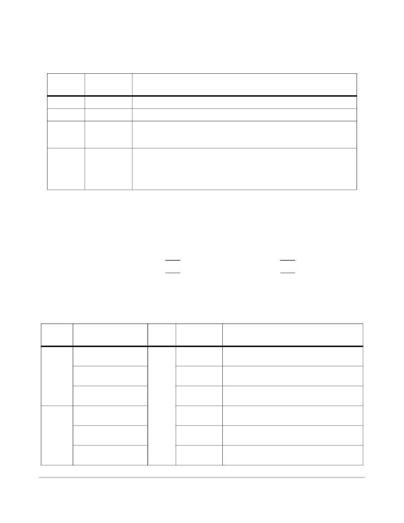
�Table� 6-5.� SIU� Register� Programming�
�Register�
�RMR�
�IMMR�
�SYPCR�
�BCR�
�Init�
�Value[hex]�
�0001�
�04700000�
�FFFFFFC3�
�100C0000�
�Description�
�Check-Stop� Reset� enabled.�
�Internal� space� @� 0x047000000�
�Software� watchdog� timer� count� -� FFFF,� Bus-monitor� timing� FF,� PPC� Bus-monitor� -�
�Enabled,� Local� Bus-monitor� -� Enabled,� S/W� watch-dog� -� disabled,� S/W� watch-dog�
�(if� enabled)� causes� reset,� S/W� watch-dog� (if� enabled)� -� prescaled.�
�Single� PowerQUICC� II,� 1� wait-states� on� address� tenure,� No� L2Cache,� 1� clock� hit�
�delay� (when� L2cache� available),� 1-level� Pipeline� depth,� Extended� transfer� mode�
�enabled� for� PCC,� Extended� transfer� mode� disabled� for� Local� Buses,� Odd� parity� for�
�PPC� &� Local� Buses,� External� Master� delay� enabled,� Internal� space� responds� as� 64�
�bit� slave� for� external� master� (not� relevant� for� this� application).�
�6.2.2�
�Memory� Controller� Register� Programming�
�The� memory� controller� on� the� MPC8272ADS� is� initialized� to� 100MHz� operation,� that� is,�
�the� registers’� programming� is� based� on� 100-MHz� timing� calculation.� It� also� works� for�
�slower� bus� speeds,� but� the� timing� must� be� optimized).� The� two� possible� initialization� for�
�the� memory� controller� are� the� following:�
�?�
�?�
�Flash� SIMM� is� assigned� to� CS0� and� E� 2� PROM� is� assigned� to� CS4.�
�Flash� SIMM� is� assigned� to� CS4� and� E� 2� PROM� is� assigned� to� CS0.�
�Both� options� are� shown� in� Table� 6-6� and� Table� 6-7,� respectively.�
�Table� 6-6.� Memory� Controller� Initialization� For� 100MHz—Flash� as� Boot� Device�
�Reg.�
�BR0�
�Device� Type�
�SM73228XG1JHBG0� by�
�Bus�
�PPC�
�Init� Value�
�[hex]�
�FF801801�
�Description�
�Base� at� FF800000,� 32� bit� port� size,� no� parity,�
�Smart� Modular� Tech.�
�GPCM�
�SM73248XG2JHBG0� by�
�Smart� Modular� Tech.�
�SM73288XG4JHBG0� by�
�Smart� Modular� Tech.�
�FF001801�
�FE001801�
�Base� at� FF000000,� 32� bit� port� size,� no� parity,�
�GPCM�
�Base� at� FE000000,� 32� bit� port� size,� no� parity,�
�GPCM�
�OR0�
�SM73228XG1JHBG0� by�
�Smart� Modular� Tech.�
�SM73248XG2JHBG0� by�
�Smart� Modular� Tech.�
�SM73288XG4JHBG0� by�
�Smart� Modular� Tech.�
�FF800876�
�FF000876�
�FE000876�
�8MByte� block� size,� CS� early� negate,� 11� w.s.,�
�Timing� relax�
�16MByte� block� size,� CS� early� negate,� 11� w.s.,�
�Timing� relax�
�32MByte� block� size,� CS� early� negate,� 11� w.s.,�
�Timing� relax�
�Chapter� 6.� Memory� Map�
�发布紧急采购,3分钟左右您将得到回复。
相关PDF资料
MPC8308-RDB
BOARD REF DESIGN MPC8308
MPC8309-KIT
KIT EVALUATION FOR MPC830X
MPC8315E-RDB
PROCESSOR BOARD PWRQUICCII PBGA
MPC8349E-MITX-GP
KIT REFERENCE PLATFORM MPC8349E
MPC8349E-MITXE
BOARD REFERENCE FOR MPC8349
MPC8377E-MDS-PB
BOARD MODULAR DEV SYSTEM
MPC8569E-MDS-PB
BOARD MOD DEV SYSTEM MPC8569
MPC8572EAMC
MPC8572 AMC RAPID SYSTEM
相关代理商/技术参数
MPC8272CVR
制造商:MOTOROLA 制造商全称:Motorola, Inc 功能描述:MPC8272 PowerQUICC II Family Hardware Specifications
MPC8272CVRB
制造商:FREESCALE 制造商全称:Freescale Semiconductor, Inc 功能描述:PowerQUICC II⑩ Family Hardware Specifications
MPC8272CVRE
制造商:FREESCALE 制造商全称:Freescale Semiconductor, Inc 功能描述:PowerQUICC II⑩ Family Hardware Specifications
MPC8272CVRI
制造商:FREESCALE 制造商全称:Freescale Semiconductor, Inc 功能描述:PowerQUICC II⑩ Family Hardware Specifications
MPC8272CVRM
制造商:FREESCALE 制造商全称:Freescale Semiconductor, Inc 功能描述:PowerQUICC II⑩ Family Hardware Specifications
MPC8272CVRMIBA
功能描述:微处理器 - MPU 266 MHz 505.4 MIPS
RoHS:否 制造商:Atmel 处理器系列:SAMA5D31 核心:ARM Cortex A5 数据总线宽度:32 bit 最大时钟频率:536 MHz 程序存储器大小:32 KB 数据 RAM 大小:128 KB 接口类型:CAN, Ethernet, LIN, SPI,TWI, UART, USB 工作电源电压:1.8 V to 3.3 V 最大工作温度:+ 85 C 安装风格:SMD/SMT 封装 / 箱体:FBGA-324
MPC8272CVRP
制造商:FREESCALE 制造商全称:Freescale Semiconductor, Inc 功能描述:PowerQUICC II⑩ Family Hardware Specifications
MPC8272CVRPIEA
功能描述:微处理器 - MPU 300 MHz 570 MIPS
RoHS:否 制造商:Atmel 处理器系列:SAMA5D31 核心:ARM Cortex A5 数据总线宽度:32 bit 最大时钟频率:536 MHz 程序存储器大小:32 KB 数据 RAM 大小:128 KB 接口类型:CAN, Ethernet, LIN, SPI,TWI, UART, USB 工作电源电压:1.8 V to 3.3 V 最大工作温度:+ 85 C 安装风格:SMD/SMT 封装 / 箱体:FBGA-324